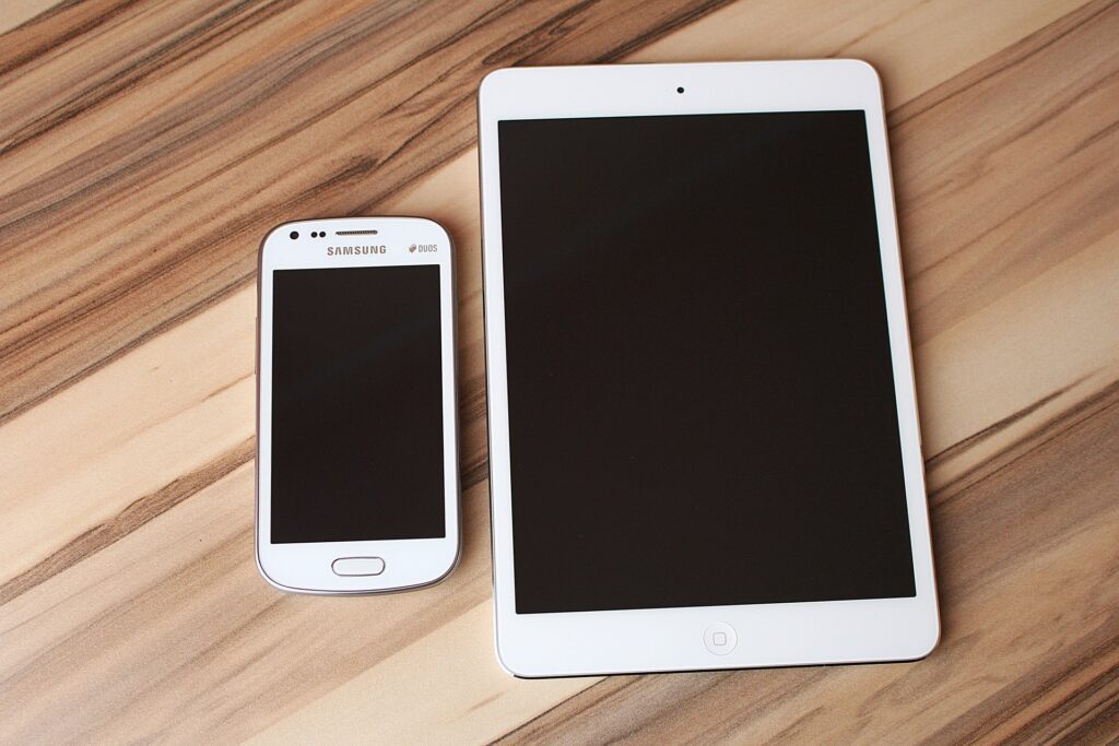
Your phone, tablet, and smartwatch all have one thing in common: they all contain a Printed Circuit Board.
Before the invention of the circuit board in 1936, all electronic devices were constructed using point-to-point wiring. Point-to-point wiring is hard to manufacture on a large scale and takes a great deal of money and skill to complete. It is also not very space-efficient.
Printed Circuit Boards essentially contain and map circuits on an easily replicable slab. They are used in almost all modern electronic devices apart from extremely simple examples. Typically, a Printed Circuit Board is made up of a layer (or multiple layers) of conductive material wedged in between plastic coatings. Holes are then drilled into the board, and components such as transistors, inputs, outputs, and capacitors can be inserted into the holes, put into contact with the conduit, and affect the electrical circuit that flows through it. More modern components do not need to be inserted directly into the board: they can sit on top of it, allowing for non-disruptive removal and replacement. These are the kind of components you would see if you took your phone apart.
What follows is a quick guide to the different kinds of PCB that form the hearts of our tech. If you are a budding tech repair hobbyist on a PCB search for a board that fits your specific device, take a look at the Octopart website.
Single-Sided
Single-sided Printed Circuit Boards only have one conductive layer and can contain components on only a single side. They are very cheap and typically quite simple in appearance. Circuits are easily mapped on these boards, which makes them very popular with hobbyists or people making their first circuit board builds. You won’t find this kind of board in your phone or tablet: they are a bit too limited for complex miniature devices.
Multilayer
Complex electronic devices require lots of componentry to fulfill their roles. In order for component heavy devices to remain small, multilayered Printed Circuit Boards had to be developed that allowed for the operation of compact, complex circuits that were not compromised by the electromagnetic interference that plagued component heavy electronics. Electromagnetic interference is the disturbance caused by one electronic device to another when they are activated in close proximity. In the 1960s, multilayer Printed Circuit Boards were designed with special insulation between layers in order to combat interference. In the digital age, multilayer PCB design has become the norm.
Flexible
Flexible Printed Circuit Boards are rather more expensive to produce than their rigid equivalents, but they have some unique applications. In devices where space and weight are awkwardly constrictive – like satellites – flexible Printed Circuit Boards allow designers to split boards into different zones without using wiring. The substrate in flexible PCBs is made of thin plastic.
Rigid
The huge majority of Printed Circuit Boards are, however, rigid. Rigid boards suit automated manufacture – robotic construction machines can easily be programmed to assemble devices based around rigid PCBs because their parameters are assuredly uniform.


